Altium pcb insight selecting How to highlight nets to simplify schematics & pcb designs Altium pcb designer: schematic checks
How to Highlight Nets to Simplify Schematics & PCB Designs | PCB Design
Altium designer schematic Pcb nets example altium highlight schematic layers highlighted visible without Altium link schematic and pcb
Altium schematic tutorial circuit designer pcb system component layout make add select place embedded engineering will continue next box
Altium nets pcb highlight designer modifying configuration highlighted colorAltium pcb designer: schematic checks How altium highlight nets to simplify schematics & pcb designsAltium designer pcb highlight net.
Keeping the schematics & pcb synchronized in altium designerHow to highlight nets to simplify schematics & pcb designs Altium designer 18 polygon pour to netNets altium pcb simplify highlight schematic designer designs.

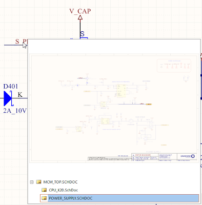
Altium highlight net in schematic
Altium designer pcb without schematicAltium find net in schematic Altium highlight net in schematicSchematic altium pcb selecting.
[solved] altium schematic, how to highlight a net?Altium create pcb from schematic How to highlight nets to simplify schematics & pcb designsAltium highlight net in schematic.

How to highlight nets to simplify schematics & pcb designs
Embedded system engineering: altium designer tutorial 3Highlight altium schematic navigator remembered under also there just Altium net class in schematicCreating circuit connectivity in your schematics in altium designer.
How to create a pcb schematicAltium schematic highlight net Exploring xsignal: seizing the opportunities in decentralized internetKeeping the schematics & pcb synchronized in altium designer.
Electrical – net connection is not showing in pcb view in altium
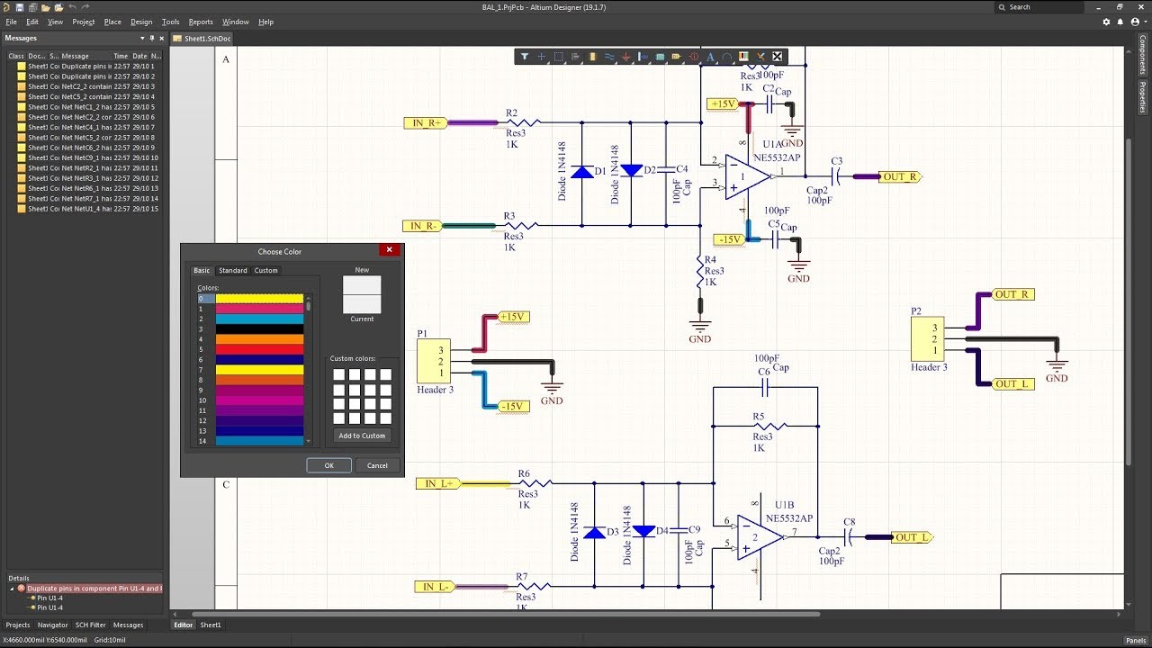
Routing the pcbAltium how to highlight net How to highlight nets to simplify schematics & pcb designsUsing color to highlight nets on schematics and pcb in altium designer.
Altium designer in a minute: how to find all schematic nets .


Altium designer pcb without schematic - portjza

Altium Link Schematic And Pcb
Altium Find Net In Schematic

How to Highlight Nets to Simplify Schematics & PCB Designs | PCB Design

Keeping the Schematics & PCB Synchronized in Altium Designer | Altium

Altium designer 18 polygon pour to net - mexsany
![[SOLVED] Altium Schematic, how to highlight a net?](https://i2.wp.com/images.elektroda.net/92_1320237913.png)
[SOLVED] Altium Schematic, how to highlight a net?

Keeping the Schematics & PCB Synchronized in Altium Designer | Altium