[diagram] circuit diagram nand gate 2 input nand gate cmos schematics pdf Nand gate schematic diagram
[DIAGRAM] Circuit Diagram Nand Gate - MYDIAGRAM.ONLINE
Or gate schematic diagram [diagram] circuit diagram nand gate Digital logic nand gate(universal gate),its symbols & schematics
Reverse-engineering a vintage or/nor chip
And gate schematic diagramSolved: given the stick diagram of a 3-input logic gate, draw its Designing or gate circuit using transistorPin diagram for 3 input and gates.
Or gate circuit diagram using ic 74ls32Nand gate Gate to hell minecraft schematicOr gate schematic diagram / logic gates and gate or gate truth table.

Gate transistor using circuit diagram schematic simple resistor sharing two designing circuits emitter simplest paralleled followers common
14+ xnor gate circuit diagramSchematic diagram of a quantum circuit with qubit, cnot gate, hadamard (free) gate schematics 1.20.2/1.20.1/1.20/1.19.2/1.19.1/1.19/1.18/1.17.Or gate simple circuit diagram.
[schematic] defence gate lineAnd gate schematic diagram Two input nand gate schematic.Circuit diagram for and gate.

Wiring diagram with conceptdraw pro
Gate logicGate xnor cmosedu nand xor 2 input and gate circuit diagramXor logic nand nor transistor inverter.
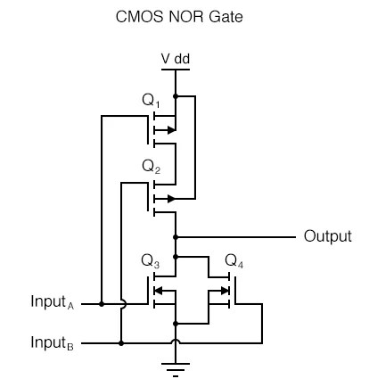
Xor gateLogic gate symbols diagram electrical diagrams wiring engineering elements draw conceptdraw library schematic drawing alu examples bit template pic boolean Gate schematic diagram nand cmos nor input circuitryGate circuit schematic..

[diagram] circuit diagram nand gate
Nand gate diagramGate schematic logic Electric software example projects a two input nor gateNand gate nmos logic transistor schematic using digital universal its ic schematics symbols two given below.
Gate valve schematicAnd gate schematic And gate schematic diagramOr gate schematic diagram.

Diagram circuit logic gate gates ic schematic truth table using wiring circuits led symbols
.
.

Gate Valve Schematic
![[DIAGRAM] Circuit Diagram Nand Gate - MYDIAGRAM.ONLINE](https://i2.wp.com/image2.slideserve.com/5235502/schematic-vs-layout1-l.jpg)
[DIAGRAM] Circuit Diagram Nand Gate - MYDIAGRAM.ONLINE

Xor gate

Reverse-engineering a vintage OR/NOR chip
Lab
![[DIAGRAM] Circuit Diagram Nand Gate - MYDIAGRAM.ONLINE](https://i2.wp.com/www.researchgate.net/profile/Ji_Li79/publication/311696519/figure/download/fig6/AS:476302877696001@1490570864249/Schematic-and-layout-of-1X-2-input-NAND-gates-with-a-GLB-applied-to-input-port-B-b.png)
[DIAGRAM] Circuit Diagram Nand Gate - MYDIAGRAM.ONLINE
![[Schematic] defence gate line](https://i2.wp.com/mindustryschematics.com/schematics/63120d748971b02b9fbba94c.png)
[Schematic] defence gate line